


How are semiconductors fabricated? | Explained Premium
The Hindu
Semiconductors, the foundation of modern technology, shape our daily lives and hold the key to future innovations. This article explains how they are made.
While the physical realm of human activity contains an array of languages, the digital realm is founded on just one fundamental binary language: the 1s and 0s, also called the bits of data. Computers represent these bits as electrical signals and this forms the foundation of modern computing, communication, social media, robotics, and artificial intelligence. The 0s and 1s constantly shape the way we interact with technology and with each other on a daily basis – and the beating heart of this binary revolution is the semiconductor device.
Semiconductors represent a distinct class of materials that possess some of the electrical properties of both conductors and insulators. Like a faucet can be used to control the flow of water, semiconductors can be used to control the flow of electric currents, and with exquisite precision.
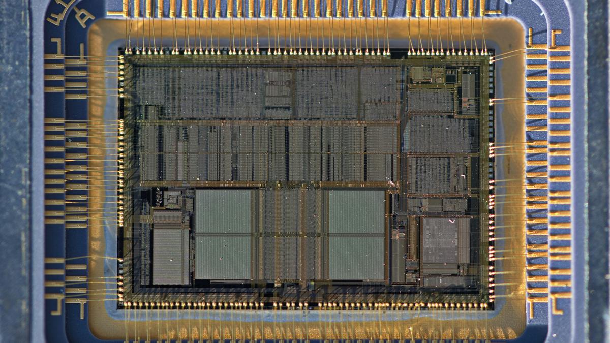
The most important type of a semiconductor is the transistor. At the dawn of the era of modern electronics, the first integrated circuits featured four transistors. Together, they controlled the flow of currents in such a way that the circuits could perform simple arithmetic operations. Today, we have single chips boasting billions of transistors.
Fitting so many transistors on a tiny chip no bigger than a fingernail requires extreme precision and a microscopic eye for detail. For instance, the accuracy required is equivalent to dividing a strand of human hair into a thousand segments each of specific width, and further subdividing each segment into a hundred parts. This is why fabricating semiconductors involves cutting-edge technology and science.
The process starts with an engineer carefully selecting a silicon wafer as the foundation on which the semiconductor will be built. A team puts silicon, sourced from sand, through a meticulous purification process to separate it from other substances, until they have an ultra-pure wafer with impurity levels as low as a few parts per billion. (This percentage is comparable to an error of merely 1 cm when measuring the earth’s diameter.)
Next is the photolithography process – a crucial step that carves the circuit pattern on the wafer. The wafer is coated with a light-sensitive material called a photoresist. Then, a mask is held in front of the wafer and light is shined on it. The mask contains small gaps in the shape of the circuit pattern. The light passes through these gaps and erodes the underlying parts of the photoresist. As a result, the photoresist on the wafer ‘acquires’ the pattern of the transistor circuits.
Following photolithography, engineers use chemical and/or physical techniques to remove the uncarved parts of the photoresist, leaving behind the circuit’s structure on the silicon substrate.
 Run 3 Space | Play Space Running Game
 Traffic Jam 3D | Online Racing Game
 Duck Hunt | Play Old Classic Game
Exploring the quest for alien life through Bayesian analysis, emphasizing the importance of asking the right questions in research.

ANRF offers Prime Minister Professorships with ₹30 lakh fellowship for retired scientists to mentor emerging research at State universities.

Unraveling the impact of cysteine deficiency on rapid weight loss, highlighting the importance of amino acids in nutrition.

Indian astronaut Group Captain Shubhanshu Shukla completes 7 microgravity experiments during 18-day stay at ISS, returning to Earth.

Filmmaker Peter Jackson partners with Colossal Biosciences to genetically engineer extinct moa birds, sparking scientific and ethical debates.

Deserts are not failures, but ancient, diverse ecosystems needing protection and respect from human interventions and policies.

Indian astronaut Group Captain Shubhanshu Shukla describes India from space as ambitious, fearless, confident, and full of pride.

Discover monsoon treks in the Eastern Ghats near Visakhapatnam, offering scenic trails, cultural immersion, and challenging adventures for all levels.

Alzheimer's disease progression linked to microglia fat metabolism, potential new treatment target identified in recent study.

On July 13, 1995, NASA’s Galileo spacecraft released the atmospheric entry probe that it carried. A.S.Ganesh tells you more about this mission with particular emphasis on the probe, which hit Jupiter’s atmosphere in December 1995.

Prada collaborates with local artisans in Maharashtra to launch 'Made in India' leather sandals, addressing cultural appropriation concerns.

Discover the rising demand for 2.5 BHK homes in Indian cities, offering flexibility and value for modern living.

Ranga Shankara’s Theatre for Children Festival returns to Bengaluru